Here the pattern in the photoresist is transferred to the underlying chip using Hydrofluoric acid (HF).
The chip has a surface layer of SiO2. Where the SiO2 is not covered by the photoresist,
the HF etches it away. The patterned SiO2 is then used to control where "dopant" impurities and metal
will contact the silcon wafer below.
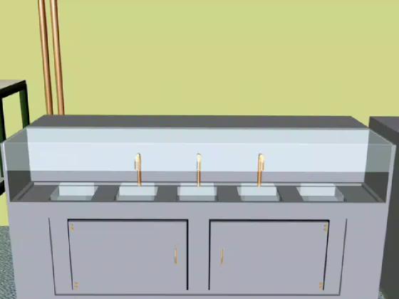
HF is highly corrosive (and attacks nerve fibers)! The wetbench is designed to eliminate contact with HF -
but extreme care must nevertheless be taken!!